4 Şubat 2015 Çarşamba


8 Nisan 2012 Pazar
4 Mart 2012 Pazar
27 Haziran 2011 Pazartesi
Rollerball writes electronics straight to paper
Electronic circuits can be fiddly to make: engineers have to snap components onto a board or etch designs onto a copper surface. Now a US group of researchers has demonstrated that all you really need is a pen and some paper.
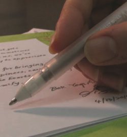
A regular, shop bought rollerball pen was filled with conductive ink © Advanced Materials / Wiley VCH |
There has been a lot of interest in so-called desktop electronics manufacturing in recent years. Researchers have demonstrated that, using conductive ink, it is possible to create circuits using airbrushes or even inkjet printers. As a result, devices such as LED displays, antennae and even batteries have been printed onto various surfaces, from fabric to paper.
The pen-on-paper technique might be the most straightforward and accessible method yet. Lewis's group made a conductive ink from silver nanoparticles, produced in solution by reducing silver nitrate and using a capping agent (poly-acrylic acid) to prevent the particles growing too big. The researchers then removed the capping agent and tailored the viscosity of the ink by adding hydroxyethyl cellulose, before loading it into a store bought rollerball pen.
Using this pen, Lewis's group was able to draw working circuits for an LED display and an antenna, which they folded into a spherical shape. At times, the components had to be attached using an extra blob of ink and superglue, but at other times the only tools necessary were the pen and paper, says Lewis. Once dry, the researchers found that they could bend the paper circuits several thousand times before any breaks appeared.
Henning Sirringhaus, a specialist in microelectronics at the University of Cambridge, UK, and chief scientist at Plastic Logic, a technology start-up company commercialising printed organic transistor technology, says it is a 'novel approach'. But he doubts whether it could create high-resolution or highly integrated circuits. Still, he says the method 'offers very interesting opportunities for simple applications of flexible electronics on paper substrates.'

The system can be used for conductive electronic art drawn on Xerox paper © Advanced Materials / Wiley VCH |
In fact, Lewis's group has shown that it can write the conductive ink on other surfaces besides paper, such as polymer films, wood and ceramics. The next step for the researchers is to expand their ink palette to include other conductive substances. 'This is an important step towards enabling desktop manufacturing using very low cost, ubiquitous printing tools,' says Lewis.
Jon Cartwright
Interesting? Spread the word using the 'tools' menu on the left.
References
A Russo et al., Advanced Materials, 2011, DOI: 10.1002/adma.201101328Chemistry News Articles: 'Artificial leaf' moves closer to reality
23 Haziran 2011 Perşembe
Properties of 'confined' water within single-walled carbon nanotube pores clarified
Properties of 'Confined' Water Within Single-Walled Carbon Nanotube Pores Clarified
ScienceDaily (June 22, 2011) — Water and ice may not be among the first things that come to mind when you think about single-walled carbon nanotubes (SWCNTs), but a Japan-based research team hoping to get a clearer understanding of the phase behavior of confined water in the cylindrical pores of carbon nanotubes zeroed in on confined water's properties and made some surprising discoveries.
The team, from Tokyo Metropolitan University, Nagoya University, Japan Science and Technology Agency, and National Institute of Advanced Industrial Science and Technology, describes their findings in the American Institute of Physics' Journal of Chemical Physics.
Although carbon nanotubes consist of hydrophobic (water repelling) graphene sheets, experimental studies on SWCNTs show that water can indeed be confined in open-ended carbon nanotubes.
This discovery gives us a deeper understanding of the properties of nanoconfined water within the pores of SWCNTs, which is a key to the future of nanoscience. It's anticipated that nanoconfined water within carbon nanotubes can open the door to the development of a variety of nifty new nanothings -- nanofiltration systems, molecular nanovalves, molecular water pumps, nanoscale power cells, and even nanoscale ferroelectric devices.
"When materials are confined at the atomic scale they exhibit unusual properties not otherwise observed, due to the so-called 'nanoconfinement effect.' In geology, for example, nanoconfined water provides the driving force for frost heaves in soil, and also for the swelling of clay minerals," explains Yutaka Maniwa, a professor in the Department of Physics at Tokyo Metropolitan University. "We experimentally studied this type of effect for water using SWCNTs."
Water within SWCNTs in the range of 1.68 to 2.40 nanometers undergoes a wet-dry type of transition when temperature is decreased. And the team discovered that when SWCNTs are extremely narrow, the water inside forms tubule ices that are quite different from any bulk ices known so far. Strikingly, their melting point rises as the SWCNT diameter decreases -- contrary to that of bulk water inside a large-diameter capillary. In fact, tubule ice occurred even at room temperature inside SWCNTs.
"We extended our studies to the larger diameter SWCNTs up to 2.40 nanometers and successfully proposed a global phase behavior of water," says Maniwa. "This phase diagram (see image) covers a crossover from microscopic to macroscopic regions. In the macroscopic region, a novel wet-dry transition was newly explored at low temperature."
Results such as these contribute to a greater understanding of fundamental science because nanoconfined water exists and plays a vital role everywhere on Earth -- including our bodies. "Understanding the nanoconfined effect on the properties of materials is also crucial to develop new devices, such as proton-conducting membranes and nanofiltration," Maniwa notes.
Next up, the team plans to investigate the physical properties of confined water discovered so far inside SWCNTs (such as dielectricity and proton conduction). They will pursue this to obtain a better understanding of the molecular structure and transport properties in biological systems.

22 Haziran 2011 Çarşamba
Chemistry News Articles: New insights on an old material will enable design...
Chemistry News Articles: New catalyst will allow commercialization of revol...
Chemistry News Articles: Nanotechnology circuits for wireless devices: Firs...
Chemistry News Articles: Chirality: New method to consistently make left-ha...
4 Aralık 2010 Cumartesi
Selam Windowslu Biz Dostuz. Barış İçin Geldik.

Bakmayın burada 2009 reklamı olduğuna Pardus 2011'in alfa ve beta sürümleri çoktan çıkmış durumda. Yeni yılın ilk çeyreğinde net olarak biteceğini düşünüyorum.
31 Ekim 2010 Pazar
28 Ekim 2010 Perşembe
28 Eylül 2009 Pazartesi
27 Eylül 2009 Pazar
9 Temmuz 2009 Perşembe
9 Mayıs 2009 Cumartesi
Deyimler
2. Eli ile etti boynu ile çeksin.
3.